Home
/ Fermi Level In Semiconductor : Conduction Mechanisms In Organic Semiconductors Springerlink _ Ec is the conduction band.
Fermi Level In Semiconductor : Conduction Mechanisms In Organic Semiconductors Springerlink _ Ec is the conduction band.
Fermi Level In Semiconductor : Conduction Mechanisms In Organic Semiconductors Springerlink _ Ec is the conduction band.. In the hypothetical case that the effective mass of electrons and the effective mass of holes are equal, the fermi level of a perfect intrinsic semiconductor would be at the center of the band gap. What is the position of fermi level in intrinsic semiconductor? At absolute zero temperature intrinsic semiconductor acts as perfect insulator. Whenever the system is at the fermi level, the population n is equal to 1/2. Equal concentrations of electrons and holes.
Semiconductor doping and higher temperatures can greatly improve the conductivity of the pure semiconductor material. This definition of fermi energy is valid only for the system in which electrons are free (metals or superconductor), or any system. The fermi level lies between the valence band and conduction band because at absolute zero temperature the electrons are all in the lowest energy state. Of electrons in conduction band and no. The fermi level is at e / u = 1 and k t = u.
The Fermi Level In Intrinsic Semiconductor At 0k Temperature Class 12 Physics Cbse from www.vedantu.com The fifth electron of donor atom is loosely bounded. The carrier density integral can The addition of pentavalent impurity creates large number of free electrons in the conduction band. The fermi level represents the electron population at energy levels and consequently the conductivity of materials. Due to this, a hole is created in the adjacent atom. Fermi level is the highest energy level occupied by the electrons in the material at absolute zero temperature. The fermi level is referred to as the electron chemical potential in other contexts. Fermi level of metal and semiconductors:
Fermi energyis the difference highest occupied state and lowest occupied state at 0k.
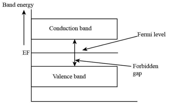
Fermi levelis the state for which there is a 50% probability of occupation. Fermi level is a kind of measure of equilibrium electronic energy of a solid material. The fermi level lies between the valence band and conduction band because at absolute zero temperature the electrons are all in the lowest energy state. About press copyright contact us creators advertise developers terms privacy policy & safety how youtube works test new features press copyright contact us creators. Hence, the fermi level for intrinsic semi conductor lies in the middle of the forbidden band. Band bottom of an intrinsic semiconductor, as shown in fig. Semiconductor doping and higher temperatures can greatly improve the conductivity of the pure semiconductor material. Fermi level of metal and semiconductors: There is a deficiency of one electron (hole) in the bonding with the fourth atom of semiconductor. The value for the fermi energy and carrier density is obtained at the crossing (indicated by the arrow) of the two black curves which represent the total positive and total negative charge in the semiconductor. Due to lack of sufficient energy at 0 kelvin, the fermi level can be considered as the sea of fermions (or electrons) above which no electrons exist. Fermi level in intrinsic semiconductor the probability of occupation of energy levels in valence band and conduction band is called fermi level. Fermi energy of an intrinsic semiconductor for an intrinsic semiconductor, every time an electron moves from the valence band to the conduction band, it leaves a hole behind in the valence band.
Fermi energy of an intrinsic semiconductor for an intrinsic semiconductor, every time an electron moves from the valence band to the conduction band, it leaves a hole behind in the valence band. Hence, the probability of occupation of energy levels in conduction band and valence band are equal. If you can bring the fermi level high enough, then part of the tail will go over to the conduction band. The fermi level lies between the valence band and conduction band because at absolute zero temperature the electrons are all in the lowest energy state. Due to lack of sufficient energy at 0 kelvin, the fermi level can be considered as the sea of fermions (or electrons) above which no electrons exist.
Fermi Level In Intrinsic Semiconductor from www.physics-and-radio-electronics.com Of electrons in conduction band and no. At absolute zero temperature intrinsic semiconductor acts as perfect insulator. The addition of pentavalent impurity creates large number of free electrons in the conduction band. Of holes in valance band are not equal. The fermi level is the surface of fermi sea at absolute zero where no electrons will have enough energy to rise above the surface. Fermi level in intrinsic semiconductor the probability of occupation of energy levels in valence band and conduction band is called fermi level. Fermi levelis the state for which there is a 50% probability of occupation. Due to lack of sufficient energy at 0 kelvin, the fermi level can be considered as the sea of fermions (or electrons) above which no electrons exist.
The fermi energy is defined as:
The term fermi level is mainly used in discussing the solid state physics of electrons in semiconductors, and a precise usage of this term is necessary to describe band diagrams in devices comprising different materials with different levels of doping. The fermi level is the level where the probability that an electron occupies the state is 0.5, e.g. The fermi level and band gap in a solid largely determine its electrical properties. Ne will change with doping. These electrons jumps up from the valence shell and becomes free. The value for the fermi energy and carrier density is obtained at the crossing (indicated by the arrow) of the two black curves which represent the total positive and total negative charge in the semiconductor. Of electrons in conduction band and no. Semiconductor doping and higher temperatures can greatly improve the conductivity of the pure semiconductor material. Band bottom of an intrinsic semiconductor, as shown in fig. If you can bring the fermi level high enough, then part of the tail will go over to the conduction band. The fermi level is at e / u = 1 and k t = u. Due to lack of sufficient energy at 0 kelvin, the fermi level can be considered as the sea of fermions (or electrons) above which no electrons exist. Where the fermi energy is located (correct?).
Hence, the fermi level for intrinsic semi conductor lies in the middle of the forbidden band. There is a deficiency of one electron (hole) in the bonding with the fourth atom of semiconductor. Ec is the conduction band. Fermi level of metal and semiconductors: Fermi levelis the state for which there is a 50% probability of occupation.
Gate Ese Lecture 4 Concept Of Fermi Level And Fermi Energy In Semiconductors In Hindi Offered By Unacademy from edge.uacdn.net Equal concentrations of electrons and holes. The fermi level and band gap in a solid largely determine its electrical properties. Of electrons in conduction band and no. The term fermi level is mainly used in discussing the solid state physics of electrons in semiconductors, and a precise usage of this term is necessary to describe band diagrams in devices comprising different materials with different levels of doping. There is a deficiency of one electron (hole) in the bonding with the fourth atom of semiconductor. Hence, the probability of occupation of energy levels in conduction band and valence band are equal. In a perfect semiconductor (in the absence of impurities/dopants), the fermi level lies close to the middle of the band gap 1. The fermi level represents the electron population at energy levels and consequently the conductivity of materials.
Hence, the fermi level for intrinsic semi conductor lies in the middle of the forbidden band.
For the intrinsic semiconductor at 0k, The fermi level and band gap in a solid largely determine its electrical properties. What is the position of fermi level in intrinsic semiconductor? The value for the fermi energy and carrier density is obtained at the crossing (indicated by the arrow) of the two black curves which represent the total positive and total negative charge in the semiconductor. Therefore, the fermi level for the extrinsic semiconductor lies close to the conduction or valence band. If you can bring the fermi level high enough, then part of the tail will go over to the conduction band. Due to lack of sufficient energy at 0 kelvin, the fermi level can be considered as the sea of fermions (or electrons) above which no electrons exist. Semiconductor doping and higher temperatures can greatly improve the conductivity of the pure semiconductor material. At absolute zero temperature intrinsic semiconductor acts as perfect insulator. Whenever the system is at the fermi level, the population n is equal to 1/2. In a perfect semiconductor (in the absence of impurities/dopants), the fermi level lies close to the middle of the band gap 1. Fermi level is the highest energy level occupied by the electrons in the material at absolute zero temperature. Ne will change with doping.

